 You’ve been waiting for the other shoe to drop, right? The tick to finally tock? (My clock is — as usual — running a bit behind; this should be #62, but that’s another story.) Today’s tale involves electro-mechanical logic! Computing with relays rather than solid-state gates.
Rather than the tick-tock of a mechanical clock, the tock-tick of lots and lots of relays! Aisle after aisle of racks of relays, many thousands of them all clicking away like chattering insects. That’s what is (or was) inside some of those windowless buildings found in every neighborhood with local phone service.
However, today the focus is quite a bit smaller…
Long ago I went through a phase of fascination with relay-based logic, in particular as used by the telephone company to control phone switching systems. It started when I got my hands (never mind how) on two fascinating “books” — one of diagrams, one of explanatory text, both documenting an office PBX.
The diagrams were mostly schematics — lots and lots of schematics — but there were also relay flow diagrams showing what happened when a given (critical) relay “fired” (aka: operated, activated, “closed”).
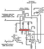
A version of a link circuit. The ‘T’ and ‘R’ lines (upper left) connect to the phone. Lifting the receiver closes the loop and activates relay ‘L’ (in red).
For example, lifting the receiver off the hook allows current to flow from the PBX (or, at home, from the Central Office or CO) through the “local loop” and your phone.
This current also flows through a relay (red rectangle in diagram to left), which closes.
That triggers a wave of hundreds of relays involved in the PBX logic to activate in ways that, nearly instantly, connect you to a Dialing Register, which sends you a dial-tone signal indicating that you may start dialing.
These early switches, unlike computers, do not operate from a stored program. There is no set of instructions telling them how to do their job. They work in virtue of how they’re wired together.
A relay-based PBX — or neighborhood CO — is just a giant, real-time logic machine complex enough to handle phone switching needs (including connecting them to long-distance trunks).
As such they’re a kind of ultimate porn for circuit-based logic junkies, especially those with a taste for the more hands-on electro-mechanical, physical systems, such as relays.

A relay.
This long introduction serves to explain why, seeking a distraction during yet another miserable Twins game, I started doodling with basic relay logic. My original idea was seeing how involved a full-adder circuit might be.
The answer surprised me, but you’ll have to wait for the punchline (or just skip to the end). Some of the in-between stuff I thought worth recording.
Casual passersby are warned the rest of this is very long and very technical. Proceed at your own risk.
§
Okay, so to start at the beginning, Boolean logic requires inversion (INV or NOT) and at least one of the basic Boolean gates.
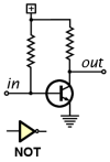
TTL NOT circuit and symbol.
One common electronic architecture (TTL) features a simple NOT circuit (left) that easily extends to a NAND gate (for more, see: Logically Speaking).
Inversion is really the key. There are passive ways to gate signals (e.g. a “wired-AND”), but inversion requires an active element, a transistor typically.
A relay also works; so does a vacuum tube (“valve” to you Brits). So would any mechanical system capable of turning a push into a pull or an up into a down.
Therefore, the first relay logic circuit that we’ll look at is an inverter or NOT circuit. This will be one cornerstone of what we’ll build (the other is how we wire the relay contacts).
This also provides a chance to introduce a way of drawing relays that might be unfamiliar even to those with experience reading electronic schematics. I learned this from those PBX books I mentioned.

Typical relay symbol.
The usual way of drawing a relay (shown to the right) typically represents the relay coil and core in a traditional way (like a transformer).
The contacts are, likewise, traditional switch symbols and — crucially — shown adjacent to, and connected with, the coil.
This last fact turns out to be extremely limiting with complex relay logic. Diagrams become mare’s nests of crossing wires.
To get around this, The Phone Company devised a much simpler symbol system that allows contacts to be placed as far away from the coil as needed.
The relay coil is drawn as just a box (easy to draw). That’s not a big stretch. What’s really different is how the contacts are drawn.
Rather than the usual switch-like symbol, a “make” contact is shown as an “X” over a wire, and a “break” contact is a straight line. A make-break (double-throw) contact has both.
Because the relay contacts may be drawn anywhere on the schematic, each are labeled with the relay’s “name” and a number signifying which set of contacts (relays usually come with two, four, or even more sets of contacts, all of which are make-break).

Fig. 1 Relay inverter-buffer.
In figure 1 (left), the relay coil is the gray box (named A). One side of the coil is shown as connected directly to the power rail.
The other side connects to an input (labeled a). A ground at that input activates the relay.
One set of Relay A contacts switches ground between the outputs A and ~A (the latter is intended to be read not-A).
When the relay is inactive, ground flows through the break contact (A-1) to the ~A output. When the relay is active, ground can flow through the make contact to the A output.
The input a, relay A, break contact A-1, and output ~A comprise an inverter! If no ground is provided to a, then ground is provided at ~A (and vice versa).
If we use, instead, output A, then we just have a buffer. A ground at a causes a ground at A.
§
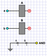
Fig 2. Relay AND circuit.
Now that we have an inverter, we can consider a logic gate. Let’s start with an AND gate. (Logically speaking, a NOT plus the AND gives us everything!)
Figure 2 (right) shows a relay AND circuit.
As with any AND, there are two inputs (a and b). In this simple circuit, each connects to its own relay (A and B, respectively).
A ground at either input activates the respective relay.
Shown below the relays is a ground path to an output (labeled AND). This ground path is broken by two make contacts (A-1 and B-1), one from each relay.
Obviously, both relay A and relay B must activate for the ground path to appear at the output. If either (or both) A or B is not active, there is no output.
§

Fig 3. Relay OR circuit.
Figure 3 shows a relay OR circuit.
The only difference is how we wire the contacts.
Now we want a ground at either a or b to give us a ground at the output (labeled OR).
So, rather than wire them in series, we wire them in parallel. It’s that simple.
The basic technique shown in these two examples carries forward to a variety of other two-input logic gates.
By using different combinations of series and parallel wiring — and by using break (inversion) contacts in addition to make contacts — we can create any two-input logic gate desired (even odd-ball ones not found in typical integrated circuit packages).
Generally speaking, a series wiring suggests AND while a parallel wiring suggests OR. However, it gets more interesting when you use break contacts.
§

Fig 4. A and not-B gate.
For example, figure 4 shows an odd-ball gate that requires activating relay A but not relay B.
There is no standard name for such a gate, so the output is labeled as A.~B (a AND not-b — as mentioned, the tilde (~) means “not” and here the dot means “and”).
Consider what we’d have if we used the break contact of relay A rather than the make contact:
That would give us not-a AND not-b.
Logically, that is identical to not (a OR b), which is the logic of a NOR gate.
Conversely, if we used break contacts in the OR circuit (fig 3) we’d implement the logic of not-a OR not-b, which logically is identical to not (a AND b), and that is the logic of a NAND gate.
§
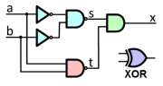
IC XOR gate and symbol.
So now we have nearly all the Boolean logic gates: NOT, AND, OR, NAND, and NOR.
There is yet one missing: XOR (exclusive-OR).
The logic of an XOR (usually pronounced “ex-or”) is similar to an OR gate, but only outputs true if either a or b is true, but not both (hence the “exclusive” part of the exclusive-OR).
With integrated circuit logic, an XOR gate electronically is a more complicated gate; it requires multiple basic gates to implement (see one example above left).
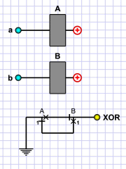
Fig 5. Relay XOR circuit.
One question I had while first playing around with this was: What does an XOR relay circuit require?
Will it require multiple relay circuits to implement?
As it turns out, a relay logic XOR is just another wiring based on what we’ve already done. Consider the actual logic of an XOR:
(a AND not-b) OR (not-a AND b)
This shows, incidentally, why an XOR requires multiple logic gates to implement. It’s an OR of two distinct AND circuits (plus some inversion).
But with relay logic, it’s just a matter of wiring contacts correctly.
We’ve already shown the (a AND not-b) circuit. The relay XOR just extends that, as shown in figure 5.
§
So, it turns out that any two-input logic gate requires just two relays and the right wiring of their contacts.
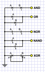
Fig 6. Relay gate module.
That leads to the interesting (if utterly impractical) idea of implementing relay logic gate “modules” that act as any type of two-input logic gate required just by selecting the appropriate output.
That is (as shown in figure 6), each module would have all the standard gates (the relays and inputs have been left off the diagram to save space, but they would be as shown on the above diagrams).
If we didn’t care about the XOR gate, the standard four gates (AND, OR, NAND, NOR) require each relay have four sets of contacts, which is pretty standard for the relays usually used.
If we have relays with six or eight, we can include the XOR gate.
Incidentally, I’ve used a system here where each relay is connected to the positive power rail and requires a ground path (presumably switched through some logic) to activate. All the logic is on the ground path side.
There’s no requirement for this; other systems work as well. I like this system because it keeps the power relatively confined to one side of the relays and involves no switching of power, as such.
Shorts in the logic wiring can cause logic errors but are not likely to cause fires.
§
Given how simple all the logic gates turned out to be, I had a suspicion that an adder circuit would likewise be easy.

Half-adder logic.
A half-adder uses just an XOR (for the sum output) and an AND (for the carry output), which has interesting implications when any two-input gate requires just two relays.
In fact, figure 6 already is a half-adder if we relabel the XOR output as sum and the AND output as carry.
A full-adder is a little more complicated. For one thing, it has three inputs because, in addition to the two bits to be added, it takes the carry output of the previous stage.

Full adder logic.
Shown right is a logic diagram for a full-adder. As you see, it requires quite a few gates.
Specifically: it requires two XOR gates, two AND gates and a single OR gate.
Logically, it can be implemented other ways, but the one shown is pretty typical.
The A and B inputs are the two bits to add. The third input, C-in, is the carry from the previous stage (or just hard-wired to logical zero if this is the first stage).
And, yet, implementing a full-adder with relay logic turns out to be rather simple:

Fig 7. Relay logic full-adder circuit.
As usual, each input has its own relay, but only three are required in total! The logic, also as usual, is in how we connect the contacts. (And we only need standard 4-pole, double-throw relays.)
The sum output (S) of a half-adder is just an XOR of the inputs. The sum output of a full-adder is an XOR if there is no carry input (Ci) but is an inverted XOR if there is a carry input. Relay C just switches between those wirings.
The carry output (Co) of a half-adder is an AND of the inputs. In a full-adder, that’s again the same with no carry input. With a carry in, carry out is an OR of the inputs, and, again, the C relay just switches between them.
§
So that’s the punchline, and if you actually read this far: BRAVO! (Also, you must be as big of an electronics geek as I am!)
But I’m not done; here’s some extra credit (which I’ll go through pretty quickly; if you’re still reading, you’re probably the type who will enjoy working some of this out yourself).
§
Computers not only have logic circuits, they also have memory circuits. And while memory circuits are usually distinct electronically, they can be implemented using logic gates.
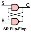 One very simple circuit is an SR-Flip-Flop, which is two gates (NAND or NOR) wired in such a way that one being true excludes the other being true, plus allows either one being true as a stable, “latched” state.
In fact, electronically, certain kinds of RAM (usually “static” RAM) does work exactly this way. Two transistors are wired in a way very similar to how the AND gates are wired. One excludes the other and two stable states exist for the circuit (hence the generic term: bi-stable circuit).
A relay version turns out to be very similar!

Fig 8. Relay SR-Flip-Flop.
Figure 8 shows a simple SR (set-reset) relay logic circuit.
To start, assume both relays are inactive. A ground at the set input activates relay S through the closed break contact R-1.
When relay S activates, make contact S-1 provides a latching path to ground that keeps S active even if the ground at the set input goes away.
Relay S stays latched unless a ground path is provided at the reset input to activate relay R. That opens contact R-1 with inactivates relay S, which also opens contact S-1 thus breaking the latch path.
Obviously, such a simple circuit requires various support circuits, but it illustrates the basic idea of a bi-stable (flip-flop) circuit.
Here’s one that’s a bit more sophisticated. It implements a D-Flip-Flop:

Fig 9. Relay logic D-Flip-Flop.
The central part of this circuit is the SR-Flip-Flop implemented with relays S and R. The wiring here is a bit different (and actually more typical) than shown in figure 8. Both the S or R relay latch to ground and both break the latch for the other relay.
As before, we can assume a start condition where both relays are inactive. (Both the SR circuit above and this D circuit therefore have a third “power on” state, which is non-ideal logically, but these are just example illustrations.)
The idea here is that a ground to the gate input allows the state of the set input to be latched into the flip-flop.
If there is a ground at the set input, relay S activates and latches. But if there is no ground, relay T (toggle) doesn’t activate, so relay R does activate and latch. The logic works regardless of whether either S or R was already active.
Here’s a rather more complicated version of a D-Flip-Flop:

Fig 10. Another D-Flip-Flop relay circuit.
Because this has gotten long (and Game #5 of the World Series is pending), I’ll leave figuring out how this circuit works as an exercise for the avid reader. The basic function is as above: activating the gate allows the D relay to latch whatever input is on the data input.
As a helpful clue, the GX relay serves to provide a delayed gate signal.
The timing diagram for this circuit is rather interesting, and someday I may return to this one with a detailed explanation. (But you know what? Probably not unless someone shows an interest. I already know how it works!)
I’ll leave you with a final kind of bi-stable circuit, a T-Flip-Flop:

Fig 11. Relay logic T-Flip-Flop.
The “T” stands for “toggle” — a T-Flip-Flop toggles back and forth between states each time the input (relay T) activates.
Essentially, this circuit consists of two SR-type circuits wired such that they interact with each other. The X-Y pair “stages” the A-B pair such that each time relay T activates, it switches the A-B pair to its opposite state.
Likewise, when relay T deactivates upon loss of ground, the X-Y pair switches state.
Note that, upon “power on” relay X will activate and latch, thus staging the A-B pair. Unfortunately, the X-Y pair in this circuit both remain off initially. The first time relay T activates, it will activate relay B (through the X-3 make contact).
Also, unlike the second D-Flip-Flop (figure 10), there are no timing considerations in this circuit.
And on that note, that’s all the relay logic I have for you now. In closing, let me just say:
GO CLEVELAND!!
Bonus: I no longer have those schematics I mentioned at the beginning (or if I do, I don’t know where they are), but as a sample of what they looked like, I found this (click for the full-sized version):


January 5th, 2021 at 10:10 am
[…] There are some especially geeky posts I’ve got planned. One about the Bell Ringer’s code (as potentially a literal code); another about the X-Bar switch (part of my fascination with telephone switching equipment and relay logic). […]
March 26th, 2021 at 7:46 am
[…] developed my understanding of phone systems in a big way. It was all relay logic, which love of I’ve written about before. (In fact, I have a post pending about the crossbar switch, which is a personal […]
September 15th, 2023 at 6:30 pm
It doesn’t seem like seven years since I published this! Time does fly when you get old!
January 9th, 2026 at 12:12 pm
[…] X-Bar switch is the pinnacle of purely electromechanical switching. Everything is accomplished with relay logic (involving thousands of […]
April 16th, 2026 at 2:16 pm
[…] the page-sized one (8½”×11″) had descriptions of the diagrams and PBX operation (see SB #61: Tock for […]
April 20th, 2026 at 9:14 am
[…] This fabric is monitored and controlled by an extremely intricate relay-logic system known as a marker. [For more on relay logic, see SB#61: Tock.] […]