 If it hasn’t been apparent, I’ve been giving a bit of a fall semester in some computer science basics. If it seems complicated, well, the truth is all we’ve done is peek in some windows. From a safe distance. And most of the blinds were down.
I thought we’d finish (yes, finish!) with a bang and take a deep dive down into the lowest levels of a computer, both on the engineering side and on the abstract logic side. When they say, “It’s all ones and zeros,” these are the bits (in both senses!) they mean.
Attention: You need to be at least this ━▇━ geeky for this ride!
When I was in high school, I learned how vacuum tubes worked only to find the world had years earlier moved mostly to transistors!
So, I learned transistors only to find that logic ICs were now a big deal.[1]
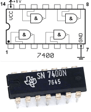
An old friend! Four whole logic gates packed into a chip less than an inch long!
So, I learned logic ICs only to find out that now I had to learn about microprocessors.
(I learned op-amps just for fun; they’re way too cool!)
Fortunately, as basic technology goes, that’s been pretty much the end of the line.
Microprocessors have gotten way better, and some associated technologies and techniques have evolved, but nothing like the earlier transitions.
Still, it’s a little mind-blowing what’s packed into modern CPU chips! Lots of architectural complexity, very dense packing of very small parts, but really pretty much the same thing as those comparatively enormous ICs with only a few logic gates.
And those were simple enough to understand in terms of their transistors, so on some level, even the most complicated CPU is just a bunch of transistors — on-off switches — arranged in really clever ways.[2]
It turns out that learning just a few basics creates a foundation that everything else is built on top of. Not only is it just ones and zeros, the whole ball of wax depends (in a way) on a single basic logic building block that is built from two even simpler logic blocks.
§
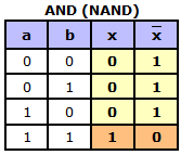
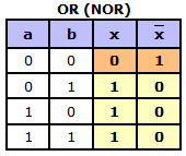
AND/NAND truth table.
The first of the two simple logic blocks is called an AND gate.
It means (logically speaking) exactly what its name implies: If this is true and that is true, the whole is true.
An AND gate is true if all its inputs are true, otherwise it’s false.[3]
The AND part of the truth table (1=true, 0=false, because binary) is the first three columns shown in the table (we’ll come back to the fourth column). The inputs (a & b) are the left two columns, the output of the AND gate (x) is column three.
 The table accounts for all possible combinations of a & b, so all possible outputs are also accounted for in the table.
The darker shading on the bottom row highlights the key fact about an AND gate: it’s true if all its inputs are true.
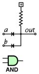
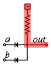
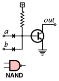
Below the table is a circuit (one of many possible) for an AND gate. Below that is one of the common block symbols for the gate (you’ll notice a similar shape in the 7400 diagram shown above).
In the circuit, the plus-in-the-box at the top is the positive power supply (aka “juice”). The jagged line (a resistor) protects the power supply by limiting how much current flows.
The arrow things are diodes. As their arrow implies, they allow current to flow only in one direction (they point the direction from plus). Their purpose is to make sure nothing can flow from a to b or vice-versa.
“0”
“1”
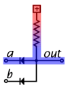
The operation is simple. If it’s just sitting there, nothing on the inputs (shown left), the output is positive (binary one) through the resistor.
But if one (or more) of the inputs provides a path to ground (shown right), current flows out the input to that ground sink. (Think of it as water in a tank draining down an open drain.) Now the output sees the ground (binary zero).[4]
AND gates are nice, but they turn out to be not that useful. All they can do is detect a unanimous yes (true) on their inputs. They can’t even detect a unanimous no (false)!
§
 We need something that little kids learn all too early: the ability to say NOT!
Logically speaking, a NOT gate just reverses the logic of its single input. (This is the only logic gate with just one input.)
A NOT gate says true is false, and false is true.
 A natural born constant contrarian!
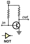
The circuit diagram and block symbol are shown below the table, and ironically for such a simple truth table, the circuit is a little more interesting!
This circuit requires a transistor (you might remember them from the Running Hot post). We need an active device to invert the logic — it can’t be done passively.
All you need to know about transistors in computers is that if current flows into the left (the base), the transistor is switched on, and current can then flow into the top right. (All that current goes out the lower right and ultimately to ground — zero volts.)
“1”
“0”
If there is nothing on the input (shown left), current can flow down the left resistor and into the base. That switches the transistor on, and current flows down the right side. The output is grounded through the transistor (binary zero).
But if the input is grounded, the current flowing down the left side is “sucked away” from the transistor base. That turns the transistor off. Now the output is positive (binary one) through the resistor.
The right-hand resistor is actually the left-hand resistor in the next stage. in fact, each stage has only one resistor. When the transistor is on, the current it sinks comes from the next stage (presumably turning off the transistor in that stage by “sucking away” its base current).[5]
We’re done. Everything from this point on builds on these two logic blocks, the AND and the NOT.
§
 If we stick a NOT after an AND, we have a NAND gate (NOT-AND).
A combination of NAND gates can make any other kind of logic gate we desire. This is based on some fundamental identities in logic.[6]
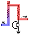
You can see that the circuit combines the AND circuit on the left and the NOT transistor on the right. A NAND is literally (electrically) an AND followed by a NOT.
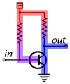
The symbol is similar to an AND, but the little circle on the output symbolizes the output NOT. It’s this NAND symbol you saw in the 7400 diagram above.
The truth table for a NAND is the fourth column in the AND/NAND table shown before. You can see it’s just the opposite of an AND gate. The bar over letter (like x) means “not x” — so x̅ is the inverse of x.
Because it embodies both the NOT and the AND principles, the NAND gate alone can create just about any logic circuit! It’s the key building block in computer logic.
Both AND and NAND gates share the property of differentiating between a unanimous true and any false. What about something that signals us on a unanimous false?
§
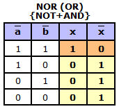
 That would be an OR gate.
The OR gate is true if any of its inputs are true, and false only if all its inputs are false.
As you might imagine, we can put a NOT after an OR to get a NOR.
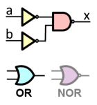
There are many ways to build an OR gate. We’re focusing on building up from AND and NOT, so we’ll stick with that for a moment.
We can invert the inputs by sending each one through a NOT first.
 Then we can use an AND gate to generate the truth table on the left (use the AND table above to see how x follows from the inverted inputs).
This exactly matches the desired OR table! (Pretty cool, eh?)
The output columns are swapped, but that’s not a problem. We just define them appropriately.
The OR gate here (fourth column) inverts both its inputs and its output. The NOR (third column), ironically, does not invert its output!
 In reality, we invert the inputs to a NAND (see right). It’s our key building block, remember. In the NAND we get the output NOT for free. This automatically swaps the columns (and now a NOR needs its output inverted).
The diagram shows the combination of two NOTs and a NAND to make an OR along with a common symbol for an OR gate (cyan).
The NOR gate (purple) adds one more NOT (three total!) as indicated by the little circle on the output.
Now we have a complimentary pair! AND gates switch between all-true and any-false. OR gates switch between all-false and any-true.
§
 We have gates that detect unanimous true and false votes. It might be useful to have a gate that detects a lone true vote.
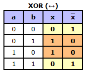
It’s called the XOR (eXclusive-OR) gate. (“ex-or”)
As the name suggests, it implements an exclusive logic. One true vote among many false, or, in the case of just two inputs: “One or the other, but not both.” The gate is true when the inputs disagree.
The inverted output of an XOR is true when the inputs agree. The XOR-NOT (There’s no name, like NXOR, for it, logically it’s called a bi-conditional) is kind of a combined AND-NOR.
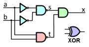 The diagram shows how to make an XOR from gates we already have. The three cyan blocks are the OR gate we just looked at.
Adding a NAND (red) and an AND (green) gives us an XOR.
If you’re wondering what it’s good for, it’s a key building block in more complex circuits (as we’ll see). It also has applications in graphics and cryptography.[7]
One of those more complex circuits is fundamental to a computer’s ability to do math.
§
 It’s called an adder. There are half-adders and full-adders. Shown right is a half-adder. It uses an XOR gate and an AND gate.
The difference between the two is that a half-adder adds two binary bits — producing a carry bit if necessary (1+1=10 in binary).
A full-adder has a third input, the carry bit from the previous adder. Computers use arrays of full-adders to do binary math.
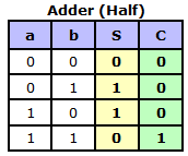 Shown right is the truth table for the half-adder. In this case we need two outputs to account for the carry bit. This truth table is binary addition.
You can see that the sum (s) is just the output of an XOR gate. The carry bit (c) is just the output of an AND gate.
That’s the thing about computers “doing math.” It’s really just simple binary logic gates, nothing more.
They can bring bits in. They can do binary logic on them; they can spit bits out. That’s it. They’re really stupid machines.
This post’s lead photo shows the truth table for a full-adder. As a reader exercise, you’re invited to come up with an arrangement of logic gates to implement it. There are several possible configurations. The highlighting is intended to provide clues.
§
 We’ll tackle one last very important piece of computer architecture: memory. There are many different types; static, dynamic, magnetic, flash, to name a few. We’ll peek at the simplest kind:
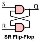
The (SR) Flip-Flop.
It consists of a pair of cross-linked NAND gates (it can also be done with NOR gates). This represents one bit of computer memory (such as you might find in a CPU register).
This is a bi-stable circuit; it has two states it can be in by itself. In one, the output (Q) is true, in the other it’s false. This post has gotten very long, so I’m going to leave figuring it out as a reader exercise (the important point is that memory is just more transistor logic).
I’ll give you this much: It’s called “SR” because the inputs are Set and Reset. The correct input on those toggles the flip-flop between conditions. See if you can work it out!
§
 Okay bottom line: Everything from here on out is just more of the same binary logic. Computers are no better than abacuses.
Their whole routine is binary logic. It’s all they know and all they can do.
Even the way they “do math” isn’t math as we commonly understand it (in fact, logic is a type of math, so it’s still math).
And that wraps up this series of posts. I’m planning a summary (almost more of an index), but I’ve pretty much said what I wanted to say.
[1] You could buy them at Radio Shack!
[2] Except for the tubes, all that early stuff turned out to be useful with modern computers. And many still prefer tubes for audio applications, so even that’s been useful.
[3] Generally we consider just two inputs (a & b), but most logic gates can be extended to more inputs while maintaining the logic of the gate.
[4] In this type of system, generally ground=zero volts=binary zero, so the positive power supply voltage is binary one. What’s more, binary zero (ground) is expected to be a “strong sink” (hole capable of draining water). Binary one, however, can be “weakly sourced” through the resistor.
[5] If you imagine the left diagram above connected to the right one, the logic is correct. The left one turns off the right one. It also works if the output of the right one wraps around to the first one’s input. The right one being off allows the left one to turn on.
[6] In fact, if you have NAND gate chips, you don’t need NOT gate chips. You just tie both inputs of a NAND gate together, and now it’s a NOT. (When you’re using chips with multiple gates, like that 7400 chip, it’s not uncommon to have some left over anyway.)
More importantly, there are two basic logical identities that we’re implementing here:
NOT (a AND b) = (NOT a) OR (NOT b)
[7] XOR has the interesting property that if apply it twice, you restore the original value. It can quickly apply and remove graphic sprites or encode and decode a message.


November 12th, 2015 at 11:18 am
I wondered if you planned to get into logic gates.
For building the OR gate, wouldn’t you have to NOT the inputs, then AND them and NOT the result? (Or NOT the inputs then NAND them?) Apologies if that’s what you described and I just got confused.
In the stuff I’ve read, usually AND, NOT, and OR are listed as the fundamental gates, I’d imagine because the wiring for a straight OR gate isn’t too complicated.
November 12th, 2015 at 12:45 pm
“I wondered if you planned to get into logic gates. “
You remembered I said maybe I would! 🙂
(It was inevitable. I really enjoyed the EE hobbyist part of my life and kind of miss it. I’ve always planned to write more about electronics here. The blog is my autobiography in a way; documents the stuff I’ve been into during my life. Hardware was a big part of it from the beginning. The software seeds planted in the 1970s eventually overgrew almost everything else!)
“For building the OR gate, wouldn’t you have to NOT the inputs, then AND them and NOT the result? (Or NOT the inputs then NAND them?)”
Correct, and that is what’s described… But I cringe every time I read that OR section. It’s poorly worded and confusing. That’s mostly because I was too lazy to redo the second truth table which shows the inverted inputs. That columns 3 & 4 are swapped is confusing.
The text does mention that the third column of that table is the NOR (not the OR as in the first table). The fourth column — the inverted output column — of the second table is the OR.
So, as you say, invert the inputs, AND them, invert the output for an OR. (Taking the uninverted output gives you the NOR.)
Or use a NAND, which gives you the output inversion “for free.” (Then you have to re-invert the output to get the NOR.)
“In the stuff I’ve read, usually AND, NOT, and OR are listed as the fundamental gates,”
Yep. That’s what’s presented here; just insert the NAND between the NOT and OR. If you start with AND and NOT, the most basic combination (one AND plus one NOT) is the NAND. The inversion of the output is the difference between AND-NAND and OR-NOR plus it’s the very identity of NOT, so inverted output is a very primal operation. (In TTL, the NAND is kind of the “natural” circuit.)
Inversion of the inputs of an AND gives a NOR, which is just as basic a single building block as is a NAND. Inversion of inputs is a secondary operation, but very fundamental logically. Inverting inputs switches the sense of the gate: AND-NOR and OR-NAND (inverting the inputs of an OR).
The inversion always gives you an “N” in the second part, but whether you invert the output or inputs controls the sense of the output logic. (I’ve always thought it was really cool how it’s a mirror image!)
A NAND [or a NOR] is a single basic block. Once you have one of those, you have everything else. Wire the inputs together for a NOT. Now you have a NAND [or a NOR] and a NOT. (Now you have a machine gun, too!) Now you have all you need.
There’s a natural logical order: AND, NOT, NAND (AND+NOT)… Now it’s dealer’s choice: NOR (NOTs+AND), OR (NOR+NOT) or OR (NOTs+NAND), NOR (OR+NOT) or even OR (NOTs+NAND), NOR (NOTs+AND).
There’s also a natural logical order: OR, NOT, NOR (OR+NOT)… etc. Mirrors images!
“I’d imagine because the wiring for a straight OR gate isn’t too complicated.”
That actually highlights what might have been my other mistake in this post. I went with TTL logic rather than CMOS because I thought a current-based story might be easier to tell than a voltage-based one.
The thing is that, in TTL, logical one and zero are qualitatively different. Logical one is a fairly high-impedance connection to the positive rail; logical zero is a (very!) low-impedance connection to ground, a current sink. In retrospect, I’m wondering if the asymmetry was confusing.
Anyway, that electrical architecture has a lot to do with wired gates. That wired-AND I started with is all you can do in TTL. But in CMOS, since you can bias both ways, you can do wired-AND or wired-OR. In CMOS both those natural orders are available.
In reality, CMOS designers mix and match to accommodate all sorts of criteria. Designing on-die is a whole other art from designing with discrete component packages.
For example, resistors in silicon require size and take up too much real estate, so instead of bias resistors on the die, they use MOSFETs wired as (low) constant-current sources. Unloaded there’s no gate voltage, so they act like huge resistors and provide bias. Loaded the gate voltage only allows the (low) constant current. It makes for weird circuit diagrams… tons of MOSFETs connected together in kind of “Hey, wait a minute!” ways and that’s about it!
Talking about this stuff… man, I really do miss it! 🙂
November 12th, 2015 at 2:37 pm
Finding a way to explain this stuff can be a challenge. Years ago, when I first learned about it, the book I read used relays as examples, similar to this HowStuffWorks article: http://computer.howstuffworks.com/boolean6.htm
I wish I knew where that book was or could remember the title. A friend of mine a few years ago wanted to learn about this stuff, and discovered that finding decent books on it is a challenge. One my engineering student workers lent him his circuits textbook, but it reportedly was too technical. (My friend has a degree in Chemical Engineering, albeit from the 70s.)
November 12th, 2015 at 5:09 pm
Ha, yeah! Relays!
Many years ago I came into possession of two associated manuals documenting a mid-sized office PBX system. About the size of several large fridges. All relay logic! (If you’re familiar with phone switching systems, it was a crossbar system.) One manual was the diagrams and “relay trees,” the other was the text descriptions of those.
Turns out Bell had its own symbols for relays and relay contacts (they use a system that allows the contacts to be scattered all over the diagram, even on other diagrams), so it took me a while to understand the schematics. Worse, they use their own jargon in the text, so that was a whole other puzzle to solve. (For instance, the circuitry in an xbar switch that manages your local loop is called a Line, Link and Marker circuit! A who now?)
What was cool (besides some really awesome relay logic involving hundreds of relays) were those relay trees. They were like family trees with the patriarch at the top and all the descendants spreading out below.
The top one would be one relay closing. The row below that, the relays that opened or closed as a result. Below that, the relevant ones affected by the second layer, and so on.
One of my favorites was the one showing, at top, the relay that closed as a result of your lifting the handset off the cradle (and drawing current through your local loop). This giant family tree of relays opening and closing (all as fast as inertial allows) so that, a dozen layers down, one particular relay ends up connecting you to dial tone (the phone company’s way of saying: I’m ready for your digits)!
For years after, I’d put my finger on the cradle button and lift the handset to my ear. Then I’d release the button and groove on the time delay to dial tone knowing what what going on. 🙂
When I was a field tech, one of my favorite clients was the phone company. I loved walking down the aisles in switching centers listening to the whisper of thousands upon thousands of relays. You can tell what kind of switching office it is by the sound!
For fun I tried making a 9-line relay logic PBX once. It worked, or rather the sub-systems all worked. When I connected them together, though, the power supply couldn’t handle the demand!
November 13th, 2015 at 12:33 pm
I really loved relays is my point… XD
(I still have boxes of them around here somewhere. Know anyone who wants a couple of hundred 24 VDC 4PDT relays?)
July 1st, 2024 at 9:01 pm
[…] logical causality of physical gates and other components comes from the electrical causality of the transistors that comprise their […]